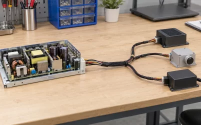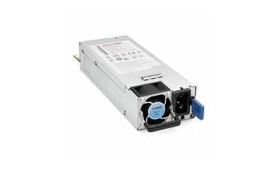
For an AI server, a CRPS module’s output voltage is an architecture choice, not a minor label on the same hot-swap cartridge. A +12 V module sends very high current through the host distribution board toward processors and accelerators. A +54 V module can carry the same transferred power at lower current across a central bus, but the system must then convert that bus to the low voltages the chips actually need. Neither output can be substituted for the other because the backplane, protection, connectors, point-of-load converters and control behavior must match the bus. “CRPS for AI” is therefore incomplete without saying which output architecture the host was built to accept.
The CRPS output is not the accelerator voltage
Accelerators, CPUs and memory require several tightly controlled voltages at their boards. The removable PSU does not normally place its main output directly on a GPU silicon rail. Power passes through a distribution assembly and local voltage-regulator stages. In a +12 V architecture, that main bus travels from the PSU bay to the load zones before local conversion. In a +54 V architecture, a higher-voltage bus travels farther into the host and conversion to lower voltages occurs nearer the consumers. The distinction is where power is transferred at high current and where conversion loss and heat are concentrated.
The Open Compute Project M-CRPS Base Specification identifies separate +12 V and +54 V main-output types in its module identification scheme. This establishes that the two outputs are distinct documented cases within that specification; it does not certify interchangeability in a particular server. The host’s approved power module, mating interface and downstream architecture still govern what can be installed. The same nominal wattage or similar enclosure outline is not enough.
This also prevents a common terminology mistake. An AC input range, a −48 V telecom input, a +54 V main output and a chip-level rail are four different locations in the conversion path. A supplier’s “54 V AI PSU” statement must say whether it describes the input or the DC output. The answer changes the PDB design. An input-side number cannot be inserted into an output-current calculation merely because the digits look similar.
Some AI platforms use other voltages or power arrangements entirely. This comparison concerns a host whose design decision is explicitly between a documented +12 V and a documented +54 V M-CRPS output implementation. It does not claim that all GPU servers use M-CRPS, or that every M-CRPS revision and vendor offers the same two choices at the same power level.
Why the central bus current changes so much
At a fixed delivered bus power, current is approximately power divided by bus voltage. For a hypothetical 3,000 W transfer, the idealized current is 250 A at 12 V and about 55.6 A at 54 V. Those numbers are arithmetic at the stated bus points, not product ratings. Real current differs with the exact power, voltage tolerance, distribution loss and operating state. The useful result is the scale of the current change: moving the central transfer point upward in voltage reduces the current that its conductors and contacts must carry.
Resistance turns current into heat according to current squared times resistance. If the same path resistance and transferred power were somehow held constant, a lower-current path would dissipate less heat. For a purely hypothetical 1 milliohm segment, the illustrated 250 A would produce 62.5 W there, while 55.6 A would produce about 3.1 W. This deliberately isolates one electrical segment; it is not a comparison of complete servers. An actual 54 V design rarely uses the same copper geometry, contacts or protection devices as a 12 V design. Engineers may trade some saved copper area for space, cost or routing flexibility, while the added downstream converters dissipate their own heat. The simple square-law illustration cannot be advertised as an end-to-end server efficiency improvement.
High current shapes a 12 V PDB physically. Copper planes, busbars, blind-mate contacts, fasteners and local branches need defined current allocation and acceptable temperature rise. A small resistance at one contact can become important when many amperes flow through it. Current sharing across parallel contacts is not guaranteed merely because they look identical. The mechanical joint, plating, contact force, board copper and cooling all matter. This is a host-interface problem as much as a PSU nameplate problem.
A 54 V central bus changes those numbers but creates different component constraints. The hot-swap and reverse-isolation devices, capacitors, bus insulation, connectors and point-of-load input stages have to be designed for that voltage and the permitted transients. Lower bus current does not allow an engineer to reuse a 12 V backplane with a different PSU plugged into it. The two systems can share a conceptual purpose—delivering energy to the same GPU workload—without sharing safe electrical interfaces.
The PDB does different work in each architecture
In a redundant server, the PDB or backplane does more than join two cartridges to a common trace. It provides a mating assembly, a route into the host loads, protection and monitoring interfaces appropriate to the platform. In a 12 V bus system, it may distribute high current through multiple heavy branches. In a 54 V bus system, it may carry less current centrally but must hand that bus to properly rated local conversion and protection stages. The board’s copper design and component ratings follow the selected voltage architecture.
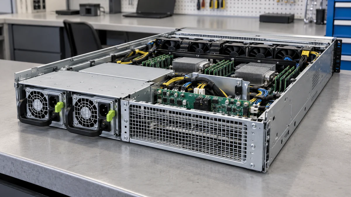
Redundant 1+1 operation does not double the protected output automatically. The single surviving module and its path must support whatever system load the platform promises after the other module or input is lost. At +12 V that failed-side condition can make a large current transfer visible at a particular mating interface or bus segment. At +54 V it changes the current and voltage stress of a different bus and its downstream input converters. A general M-CRPS label does not resolve either failure-state limit.
The host may also constrain how modules share load, enter standby, communicate status and respond to a fault. A converter that meets its own output specification on a bench can still be the wrong module for the server’s distribution and management design. For example, a compatible-looking 54 V module cannot be made into a 12 V replacement by assuming a downstream regulator is present somewhere. The needed conversion stage must actually exist in the host and be rated for the full operating and failed-module states.
Connector allocation illustrates the same point. A higher bus voltage can reduce the number of current-carrying paths needed for a given transferred power, but the permissible contact count depends on the connector design, temperature rise, redundancy scheme and standard or platform implementation. It cannot be inferred from the current ratio alone. A reduction in central copper is an engineering opportunity, not a promised property of every 54 V module.
Conversion heat moves closer to the GPU
The chip still needs low-voltage, high-current power. If the main PSU delivers +54 V, one or more downstream stages convert that bus toward the accelerator and motherboard voltage domains. Those stages occupy board space and produce heat near already dense compute zones. A +12 V architecture also uses local point-of-load regulators, but the input-stage arrangement and division of conversion loss can differ. The platform designer must allocate cooling where the loss actually occurs rather than crediting the server with a gain based only on reduced bus current.
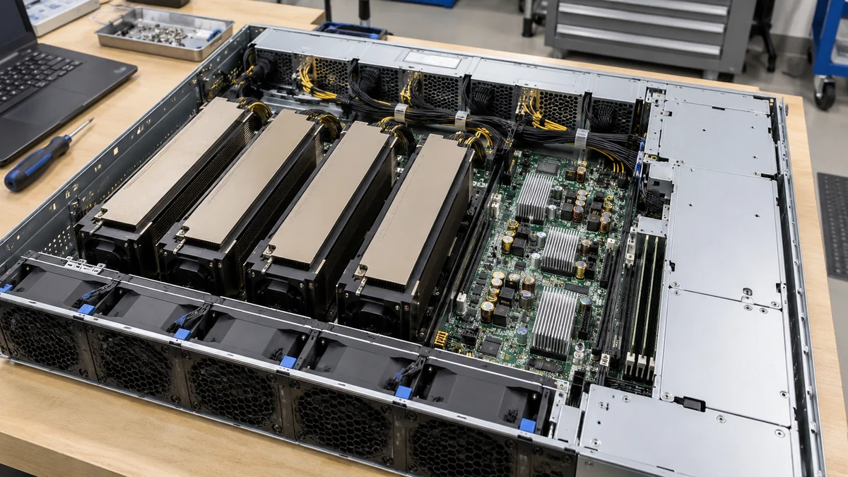
The thermal placement question is concrete in an air-cooled AI server. A DC–DC stage near GPUs may sit in a constrained air stream shared with heatsinks, memory, cables and fan walls. Placing a converter closer to a load can shorten a high-current low-voltage route; it can also raise local inlet temperature or obstruct airflow. A liquid-cooled accelerator does not automatically cool every nearby power component. The power stage may still require air or another defined thermal path. No generic “54 V runs cooler” statement survives those system details.
Transient behavior also moves. A GPU load step is initially met by local capacitance and voltage regulation, then by upstream converters and finally by the PSU and feed. A higher-voltage distribution path may reduce current in the central segment, but the extra conversion boundary has control-loop and energy-storage behavior of its own. Whether it improves or worsens the observed chip-rail response depends on the complete platform design. A PSU’s stable 54 V bench output is not evidence that the GPU rail will remain within limits during every workload transition.
Efficiency should be compared at the same endpoints. A PSU-only efficiency value measures conversion from its specified input to its main DC output under a defined test point. The GPU does not consume at that DC voltage. To compare 12 V and 54 V architectures for a workload, account for PSU conversion, PDB loss, downstream DC–DC stages and actual operating distribution. An efficient 54 V cartridge could be paired with a poor local conversion layout; a high-current 12 V bus could incur avoidable copper loss. The endpoint matters more than one badge or one intermediate bus measurement.
What is actually interchangeable?
Module outline, handle, airflow direction and CRPS-style terminology can make two cartridges appear related. Interchangeability is much narrower. The host must approve the exact main output type, electrical mating interface, capacity at the available AC or DC input, standby provisions, protection timing, cooling arrangement and management identity. A server designed around a 12 V distribution board cannot safely adopt a 54 V module through a cosmetic connector adaptation. That would put the wrong voltage into a path and load architecture built for another one.
A platform migration is different from a field substitution. An equipment designer can choose a new 54 V bus for a future AI host and redesign PDB, local converters, connectors, protection and cooling around it. That is a system architecture project. A service technician replacing a failed PSU within an existing host has no such freedom; the supported module family and configuration are the boundary. The term “upgrade” is misleading if it suggests that one output class can be swapped into another class’s backplane.
Even within one output class, power rating alone is insufficient. A higher-watt module might differ in inlet requirement, thermal operating region, depth or firmware identification. A lower-current calculation for 54 V does not override any of those constraints. Conversely, a well-supported 12 V platform is not obsolete merely because a higher-voltage topology exists. If the complete host meets its workload and failure-state contract, its distribution choice is a valid implementation rather than an error to correct.
The most useful way to read an AI-server CRPS listing is therefore to locate the bus boundary first. “+12 V output” and “+54 V output” describe two different systems between the PSU bay and the point-of-load stages. Once that boundary is known, current, copper, protection and conversion heat can be followed through the actual host. Without it, identical wattages conceal incompatible power paths.