GaN in a server power supply is a choice of power-switch technology, not a new output voltage, a certification level, or a promise that the whole PSU is more efficient. Gallium-nitride transistors can switch quickly and avoid some losses that constrain particular silicon devices. That makes them useful in selected converter stages, especially where high switching frequency or a bridgeless power-factor-correction circuit offers a real system benefit. The gain depends on the circuit around the switch. A poorly laid-out GaN stage can lose much of its theoretical advantage to ringing, electromagnetic noise, dead-time loss, cooling limits, or extra components.
Identify the stage before asking what GaN improves
An AC-input server PSU can contain several distinct power paths. The mains-input stage conditions and rectifies AC, power-factor correction (PFC) establishes an intermediate DC bus, an isolated DC-DC stage produces the main output, and auxiliary converters keep management or standby functions alive. Output isolation and protection may add further devices. Replacing a switch in one stage does not automatically change the technology or performance of the others. “GaN server PSU” is therefore too vague to explain a design until the GaN device’s location is known.
In a high-power PFC stage, GaN can be used in a fast-switching leg of a bridgeless or totem-pole arrangement. The aim is partly to avoid losses associated with a conventional input bridge and partly to switch the power devices efficiently. This is a specific topology choice, not a statement that every GaN PSU omits an input bridge. Infineon, for example, publishes a 2.5 kW GaN-based PFC evaluation board for server-supply and telecom-rectifier development. That board demonstrates a PFC stage; it is not a complete 2.5 kW server PSU with its isolated output, fan, controls, and enclosure already accounted for.
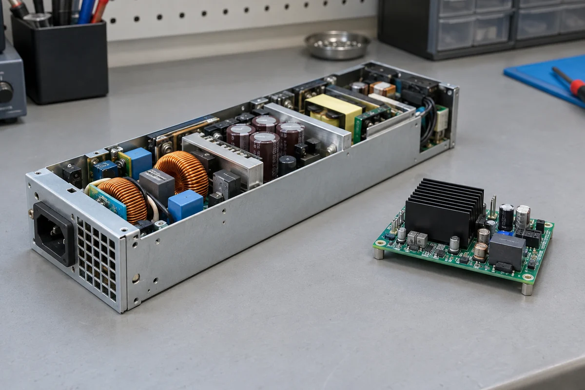
GaN may also serve in the high-voltage switching stage of an isolated converter. Faster switching can help reduce the size of a transformer or filter, but only if magnetic loss, winding construction, insulation, and heat removal remain suitable. A different application is the small auxiliary supply. Texas Instruments’ PMP23146 reference design uses a GaN half bridge in a 45 W active-clamp flyback intended to provide auxiliary power inside a server or telecom PSU. Its input comes from a PFC bus and its output is an auxiliary rail. It should not be described as a 45 W main server PSU, nor should its compact dimensions or switching frequency be assigned to unrelated full-power designs.
The distinction matters commercially. A product may use GaN only in PFC and conventional silicon in the isolated converter, or the reverse. Another may contain a GaN auxiliary supply while its main output path uses different devices. A press release calling any one of these “GaN-powered” can be accurate yet not tell a buyer which stage contributed to the claimed result. Read the identified architecture and test boundary before translating a component claim into a module-level efficiency claim.
What a faster switch actually changes
A real power switch is not an ideal on/off contact. While it changes state, current and voltage can overlap, creating transition energy that repeats at the switching frequency. The device also has capacitances that must be charged and discharged, resistance that creates conduction loss when on, and a gate that needs drive power. GaN devices can offer a favorable combination of low charge and fast transitions for a given design space. This can reduce switching loss or permit a higher operating frequency. Neither benefit is automatic across every voltage, current, and temperature point.
Higher frequency can shrink some magnetic and filter components because each switching cycle transfers energy more often. That is a route to power density, not a free efficiency multiplier. Core loss and AC winding loss may rise with frequency. The circuit may need tighter layout, different shielding, and more deliberate cooling. A designer can use GaN to make a supply smaller while holding efficiency roughly constant, to improve efficiency at a similar size, or to balance both goals. One needs the actual design result to know which trade was made.
Some silicon MOSFET arrangements face reverse-recovery loss when a diode path conducts and then has to block voltage. GaN devices do not exhibit the same minority-carrier reverse-recovery behavior, which helps explain their appeal in fast commutation paths such as totem-pole PFC. It is inaccurate, however, to call reverse conduction through a GaN device lossless. During dead time, current can flow through a reverse-conduction path with a voltage drop; excessive dead time can dissipate noticeable power. The controller’s switching sequence must capture the device benefit rather than merely install a faster transistor in an unchanged timing plan.
GaN also changes the practical limits on the gate drive. A fast transition reduces overlap time, but its steep voltage edge can excite stray inductance and capacitance in the package, board, transformer, and nearby traces. Gate-drive voltage, turn-on and turn-off impedance, dead time, overcurrent response, and protection must be matched to the chosen device. Integrated driver-and-GaN packages can shorten critical loops and simplify parts of that task, but they do not remove the need for correct board and system design.
Why the PFC example is not a whole-PSU claim
A PFC stage sits ahead of the isolated converter. If a reference board reports very high PFC efficiency, the number applies to its measured input-to-DC-bus boundary under specified conditions. The complete server PSU still loses power in its isolated stage, secondary rectification, output connector, ORing function, control circuitry, and fan. For illustration only, a hypothetical PFC at 99% efficiency followed by a hypothetical isolated stage at 96% gives about 95.0% combined efficiency before other losses: 0.99 × 0.96 = 0.9504. This arithmetic is not a measurement of an Infineon, TI, Delta, or Powernexu product.
The same boundary rule applies in the opposite direction. A GaN isolated-stage demonstration does not establish the AC-to-output performance if its PFC, filtering, cooling, and output distribution are absent from the test. If the auxiliary converter improves its own standby consumption, that can matter at light load, but it will not by itself transform the efficiency of the main high-power path. A technical comparison should identify exactly which watts enter and leave the demonstrated board.
Even within PFC, input voltage and load affect the result. At a lower AC line for the same output power, current is generally higher, so conduction losses in a given path tend to increase. At light load, control and switching overhead can dominate. A GaN-based topology may have particularly strong performance at one point and a smaller advantage at another. This does not negate the technology; it prevents a component demonstration from being misread as a fixed percentage benefit over an entire server’s operating life.
The value of the PFC example is architectural. It shows where replacing silicon with GaN can unlock a different switching arrangement and loss balance. The value is not a transferable efficiency number. A server PSU must satisfy its full input range, output regulation, transient behavior, temperature range, fault protection, acoustic constraints, and electromagnetic compatibility. The real design may choose a topology with a slightly lower peak stage efficiency if it performs better across those conditions or fits the available volume.
The fast edge makes layout part of the power circuit
At high switching speed, the shortest-looking schematic may still have a long electrical loop on the actual board. Package leads, vias, copper plane geometry, decoupling placement, gate-return routing, and transformer capacitance create parasitic paths. A large current slew through a small stray inductance can produce voltage overshoot. A high voltage slew across parasitic capacitance can send common-mode current into the chassis or cables. Both can heat components, stress insulation, or make electromagnetic emissions harder to control.
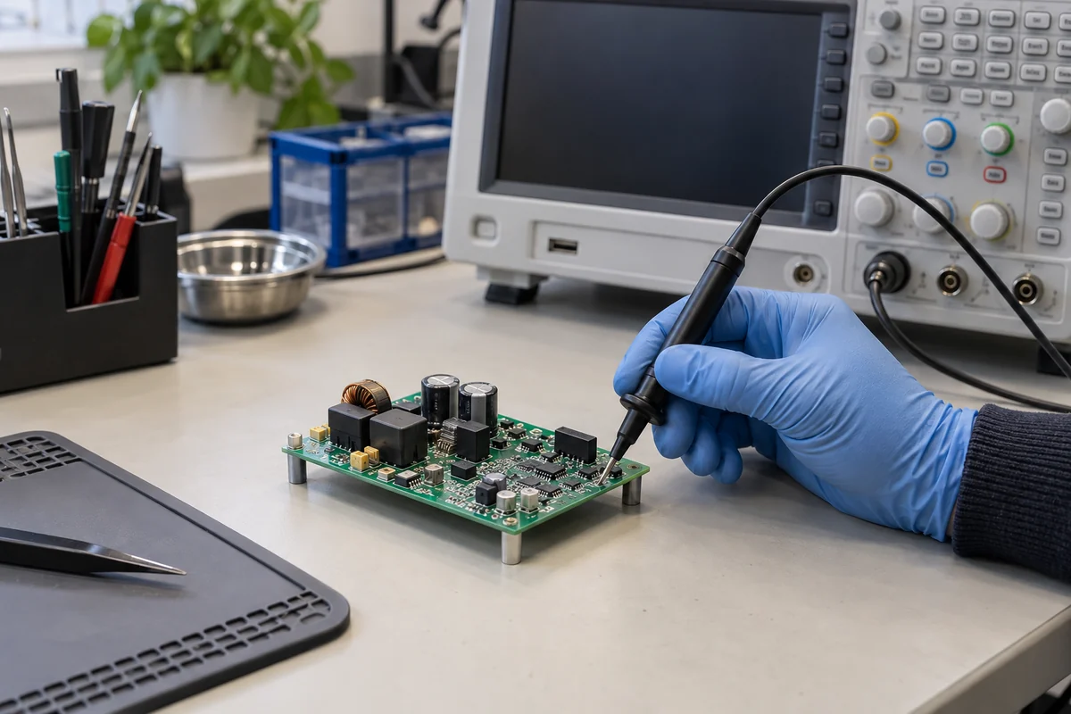
That is why a fast GaN stage is not a drop-in replacement for silicon simply because the device ratings appear compatible. The gate driver may need to sit close to the power switch. The switching loop and its local capacitor need small area. High-current returns need controlled routing. Noise-sensitive sensing and communications circuits must be separated from the power loop. The enclosure, filter, and cable arrangement still determine whether the finished PSU meets its system requirements. These are physical implementation constraints, not paperwork added after the efficiency calculation.
There is also a cost to slowing a fast switch deliberately. Gate resistors and control settings can reduce ringing and emissions by softening the edge, but they may return some switching loss. Snubbers can protect a device yet dissipate energy. Larger or additional filters can consume space that higher-frequency operation was supposed to save. A good design chooses a workable balance rather than seeking the fastest possible waveform on an oscilloscope. The optimum point depends on the whole PSU and its installation, not only the transistor datasheet.
Thermal behavior follows the same physical reality. GaN’s lower switching loss at one condition does not mean the device runs cold in every design. On-state resistance changes with temperature, heat still moves through the package and board, and a denser converter can concentrate dissipation in a smaller region. The adjacent capacitor, magnetic component, or connector may become the thermal limit even if the GaN switch has comfortable margin. Cooling requirements belong to the finished module at its specified inlet conditions.
Auxiliary power exposes a different reason to choose GaN
Why would a server designer put GaN in a 45 W auxiliary converter rather than only in a kilowatt-scale main path? An auxiliary supply can be physically constrained while it must provide isolated power for control and management functions. High-frequency operation can make a planar transformer and compact board practical. TI’s particular PMP23146 design is a useful example because its role is clearly stated: it is an auxiliary supply fed from the PFC bus, not the main AC-to-server-output converter. Its stated dimensions and operating frequency are design-specific, not a template for every PSU.
Small auxiliary power does not mean unimportant power. The controller, telemetry, communications interface, and some standby functions may operate when the main rail is lightly loaded or inactive. An auxiliary stage with avoidable no-load loss can therefore influence light-load behavior. Yet the system may need those functions continuously for fault reporting or rapid startup. The sensible aim is efficient auxiliary conversion while preserving required operation, not deleting management functions to improve an isolated test number.
GaN is one tool among several in this role. Transformer design, active-clamp control, synchronous rectification, low-loss sensing, and the input-bus conditions also shape the result. If a reference design uses all of those techniques, it would be misleading to attribute every watt saved to the transistor material alone. The circuit around GaN is part of the achievement. The same caution applies to the main converter and PFC examples: compare complete designs, not labels on semiconductor packages.
What a GaN claim can legitimately tell you
“Uses GaN” can tell an engineer that a design likely sought a particular switching-speed or power-density advantage at some point in the supply. It cannot, by itself, tell them the module’s AC-to-DC efficiency, 80 PLUS status, lifetime, failure behavior, cooling requirement, or compatibility with a server. Those properties require product-specific evidence. Conversely, a server PSU without GaN can still be highly efficient through well-designed silicon switching, magnetics, rectification, layout, and control.
The meaningful distinction is between three levels of evidence. A device datasheet describes a switch. A reference design or evaluation board demonstrates one circuit stage under its conditions. A finished PSU test describes the assembled product across its stated input and load conditions. Keeping those levels separate lets GaN’s real benefits remain visible without turning a PFC board or auxiliary converter into an unsupported promise about a complete rack system. That is where the technology fits in server power: at chosen switching nodes whose advantages survive the rest of the electrical and physical design.