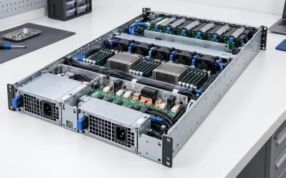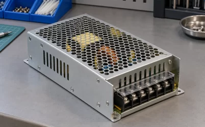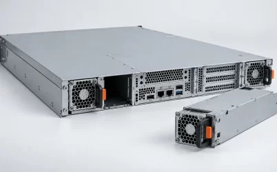
The PMBus interface pinout for a server power supply comes from the exact module documentation, not from the PMBus name. Clock, data, alert, address selection, and their electrical reference must be identified separately. Even a manufacturer document can contain inconsistent contact labels. A useful pinout therefore tells an integrator both which connections are documented and which remain unsuitable for implementation. The example here uses Murata’s D1U54P-W-450-12-HBxC connector table, with particular attention to the management contacts and an unresolved address-table reference.
This is a technical reading of that interface, not a connection procedure for an unknown PSU. It does not authorize bridging contacts, applying an external voltage, or operating a module outside its supported assembly. Readers looking for an arbitrary five-pin motherboard header will need the motherboard or power distribution board documentation as well: those header positions cannot be inferred from the PSU-side example.
The management subset of one documented card edge
Murata’s D1U54P-W-450-12-HxxC datasheet, revision A07.D03, separates the signal descriptions from the physical connector assignments. Page 4 describes the management signals. Page 6 supplies a representative gold-finger layout. Page 7 labels its assignment table specifically D1U54P-W-450-12-HBxC. That narrower heading matters: the series-level title should not silently broaden the applicability of a model-specific table.
The ordering guide identifies HB3C and HB4C variants with a 12 V standby output and different airflow directions. The following subset retains the page 7 coordinates and names. It deliberately excludes the high-current output allocation and unrelated control connections, because the search problem here is the management interface.
| Documented position | Function in the HBxC table | Important interpretation |
|---|---|---|
| S5 | SDA | Serial data, described as bidirectional |
| S6 | SCL | Serial clock, described as bidirectional |
| S7 | SMB_ALERT | Separate warning/fault output to the host |
| S17 | ADDR | Address-selection name in the connector table; a conflicting reference elsewhere needs resolution |
| P9–P16 | Main and standby output return | Return allocation identified by the connector table |
These coordinates belong to the manufacturer’s gold-finger layout. A drawing of the mating connector can present the opposite view, and a downstream header can reorder the connections. Preserve the source drawing with the table rather than turning this condensed subset into a free-standing wiring diagram. A photograph with no declared viewpoint cannot establish which visible finger is S5.
For unfamiliar hardware, Powernexu’s server PSU pinout identification article covers the broader evidence problem. Here the assignments are already available; the harder task is interpreting their electrical and addressing boundaries without extending what the document actually establishes.
The return is part of the management interface
Two named communication lines do not fully describe an electrical connection. Their logic levels require a reference. In this datasheet, the address-input description explicitly uses +VSB_Return, while the output connector table identifies P9–P16 as the main and standby output return. That is the documented return relationship available for this example. It does not assign a convenient chassis screw, shield, or remote-sense contact as a substitute signal reference.
The distinction becomes practical when a receiving controller sits on another board. Its ground label may look equivalent on a schematic, yet the physical route can include power-current voltage drop, isolation, or components. Resolve the relationship through the actual board design. An idle signal voltage measured relative to chassis can differ from the voltage that the receiving input sees relative to its own reference.
Remote-sense return also has a distinct purpose. It participates in sensing the output at the intended load point. Reusing it as a convenient communication return changes the question from locating an existing function to altering a circuit. The connector table alone supplies no justification for that alteration. Likewise, the presence contact is a detection function even where the signal description connects it internally to standby return.
A management-only harness should therefore be described by the functions it carries, their intended reference, and the receiving interface. Calling it an I²C cable does not establish those details. If the harness terminates at a server-board header, retain that header’s own position numbers and voltage specification; PSU contact names are source identities, not destination numbering.
Clock and data levels differ from alert pull-ups
The Murata signal descriptions list SCL and SDA input-low maximum at 0.8 V, input-high minimum at 2.1 V, and output-low maximum at 0.4 V while sinking 3 mA. Those values describe particular electrical conditions. The 2.1 V input-high threshold is not a recommended supply voltage, and the 3 mA condition is not a general permission to increase bus current. A receiving controller also has its own thresholds and limits.
The same page describes a series isolator on each communication line that disconnects the internal PSU bus when the module is unpowered. That is a defined module feature, not proof that an entire multi-bay backplane isolates every possible fault. External branches, controller inputs, and adapter circuitry remain outside that statement. Nor does the feature establish the behavior of a different Murata family.
A footnote recommends external pull-ups for robust communications. Its wording contains “SDA and SCA,” while the signal entries identify SDA and SCL. It also names 3.3 V or greater without supplying a complete upper-voltage permission for the proposed host interface. Neither wording should become an instruction to pull the wires to any convenient rail. Use the applicable electrical limits of the delivered module, isolator arrangement, and receiver to resolve the permitted pull-up domain.
SMB_ALERT needs separate attention. The datasheet describes an internal 10 kΩ pull-up to VDD and an open-drain output. Its VDD footnote describes an internal rail derived from standby and housekeeping sources. That rail is not established as the same supply chosen for external clock and data pull-ups. In particular, the HB variants’ 12 V standby listing makes an assumption that every management-related contact is automatically a 3.3 V signal especially inappropriate.
Before connecting an alert input, obtain its permitted voltage and the host’s receiving arrangement. An open-drain output describes how the signal is asserted; it does not establish the high-state voltage at an attached controller. A correctly located S7 contact can still meet an unsuitable receiver. Contact identity and voltage compatibility are separate results.
One analog address input selects two device identities
The address description is materially different from a pair of binary address straps. Murata describes an analog input used with an external resistor to standby return and an internal resistor-divider chain. The selection establishes addresses for two internal devices: the main controller and an external EEPROM. A pinout copied from a supply with separate A0 and A1 inputs would miss that architecture.
The address table pairs main-controller entries from 0xB0 through 0xBE, stepping by two, with EEPROM entries from 0xA0 through 0xAE. This pairing is useful evidence that “the PSU address” is an incomplete description. An identification-memory response and a power-controller response concern different endpoints, even though both reside in one removable module.
The numerical representation also needs to match the host software. A software API expecting a seven-bit device address does not accept an address byte including the transfer-direction position on the same terms. For example, if 0xB0 is confirmed as a write-address byte, its seven-bit address is 0x58 after shifting right by one. That is a conditional representation example, not confirmation of the convention used by every table or software tool.
Record the source representation and the receiving API’s expectation before converting anything. A displayed address that differs by a factor of two can reflect notation rather than different hardware. Conversely, a familiar address does not identify the bay by itself when an upstream switch determines which module is reachable. Keep route, device type, and numerical address together in diagnostic records.
A conflicting address label prevents a wiring conclusion
The document’s connector table identifies ADDR at S17. Its address-selection table then labels the resistor connection “ADDR pin (A3).” Those are different physical coordinate labels. The published text does not supply enough information here to treat A3 as a verified synonym for S17. Recognizing the intended analog-selection function does not resolve the physical inconsistency.
For that reason, this article does not reproduce resistor values as a wiring recipe or choose one label by intuition. The useful fact is the documented selection architecture; the unresolved fact is the conflicting physical reference associated with its configuration table. Ask the manufacturer for a corrected interface definition tied to the supplied HB model and revision before implementing the address resistor.
This restraint leaves the SDA, SCL, and alert entries useful as documented assignments while placing a hold on the disputed address connection. It also avoids converting an editorial error into an apparently authoritative diagram. A clean table that silently changes A3 to S17 would hide the most important information an integrator needs from the source.
An open address-input condition should not be assigned a default address from this table without further evidence either. Listed resistor configurations do not automatically define every absent, shorted, or out-of-range condition. Treat those states as unspecified here. Trial connections to discover an address would introduce electrical and control uncertainty that a documentation review is meant to remove.
Consider a hypothetical two-bay drawing review. The designer has copied the documented clock and data contacts correctly, but gives both bays one address configuration and labels the controller input simply “PMBus.” That drawing leaves two independent questions unanswered: whether both devices can be distinguished on the chosen route, and whether the receiver tolerates the actual signal levels. Correcting the contact numbers resolves neither question. Separate switched branches may change the address requirement, while a suitable receiving circuit may change the voltage interface; both need support from the actual platform design.
A manufacturer response should close the particular discrepancy, rather than merely confirm that the product supports PMBus. For this document, a useful correction identifies the intended address contact in the gold-finger coordinate system and states which delivered variants it covers. The electrical response should identify the permitted external pull-up domain and the alert output interface seen by the host. Retain that clarification alongside the original revision, because another team reviewing the same published PDF will otherwise encounter the same conflicting label. A verbal assurance that the family is standard leaves the physical coordinate and voltage questions unanswered.
What an identified PMBus contact can actually establish
Once the physical and electrical interface is supported, an acknowledged transaction demonstrates communication with an endpoint on the selected route. It does not demonstrate that the main output is enabled, that the module contributes current, or that its reported value belongs to the intended physical bay. Those questions need the command definition and the host’s association between route, address, and installation.
The separate EEPROM makes this boundary concrete. Reading memory from the module is not equivalent to successfully reading a supported measurement from its power controller. A controller identity response is also narrower than complete command compatibility. Software may reach the correct device while requesting a command or interpreting a data format that the delivered implementation does not support.
The resulting interface description has several layers: a model-specific contact allocation, a documented reference, compatible signal levels, an established addressing convention, and supported command behavior. The Murata example supplies important pieces and exposes a particular unresolved label. Keeping that gap visible gives a hardware team a precise manufacturer question instead of a plausible universal pinout that cannot safely authorize the connection.